QUATECH, INC.
SCB-1040, SCB-1050
|
Card Type |
Serial controller |
|
Chipset/Controller |
NEC |
|
I/O Options |
Serial port |
|
Maximum DRAM |
N/A |
|
CONNECTIONS | |
|
Purpose |
Location |
|
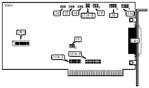
Serial port - DB-25 |
CN1 |
|
INTERRUPT SELECT - J1 | |||||||
|
Setting |
Jumper A |
Jumper B |
Jumper C |
Jumper D |
Jumper E |
Jumper F | |
| » |
IRQ4 |
open |
open |
closed |
open |
open |
open |
|
IRQ2 |
closed |
open |
open |
open |
open |
open | |
|
IRQ3 |
open |
closed |
open |
open |
open |
open | |
|
IRQ5 |
open |
open |
open |
closed |
open |
open | |
|
IRQ6 |
open |
open |
open |
open |
closed |
open | |
|
IRQ7 |
open |
open |
open |
open |
open |
closed | |
|
DMA SELECT - J2 | |||||||||
|
DMA |
A |
B |
C |
D |
E |
F |
G |
H | |
| » |
CH 1 for transmit |
closed |
open |
closed |
open |
open |
open |
open |
open |
| » |
CH 3 for receive |
open |
open |
open |
open |
open |
closed |
open |
closed |
|
CH3 for transmit |
open |
closed |
open |
open |
open |
closed |
open |
closed | |
|
CH1 for receive |
closed |
open |
open |
open |
open |
open |
closed |
open | |
|
CH1 for transmit and receive |
closed |
open |
open |
open |
closed |
open |
open |
open | |
|
CH3 for transmit and receive |
open |
open |
open |
closed |
open |
open |
open |
closed | |
|
INTERRUPT MODE | ||
|
Setting |
J3 | |
| » |
Use dedicated IRQ |
pins 1 & 4 closed |
|
Share IRQ with compatible Quatech card |
pins 2 & 5, 3 & 6 closed | |
|
RECEIVE CLOCK SOURCE | ||
|
Source |
J4 | |
| » |
Internal |
pins 2 & 3 closed |
|
External |
pins 1 & 2 closed | |
|
TRANSMIT CLOCK SOURCE | ||
|
Source |
J5 | |
| » |
Internal |
pins 2 & 3 closed |
|
External |
pins 1 & 2 closed | |
|
-SYNC/IPS SELECT | ||
|
Source |
J6 | |
| » |
Intenal synchronization mode sync notification signal enabled |
pins 2 & 3 closed |
|
External synchronization mode - sync notification signal enabled |
pins 1 & 2 closed | |
|
Asynchronous mode - general purpose signal enabled |
pins 1 & 2 closed | |
|
INTERRUPT SOURCE - J7 | |||
|
Setting |
Jumper A |
Jumper B | |
| » |
From communications controller |
closed |
open |
|
From DMA terminal count |
open |
closed | |
|
RTS/CTS MODE | ||
|
Setting |
J8 | |
| » |
RTS/CTS connected to CN1 |
pins 1 & 4, 2 & 5 closed |
|
RTS/CTS loopback enabled |
pins 1 & 2, 4 & 5 closed | |
|
HALF/FULL-DUPLEX SELECT | ||
|
Setting |
J8 | |
| » |
Half-duplex |
pins 3 & 6 closed |
|
Full duplex |
pins 3 & 6 open | |
|
RECEIVE CLOCK BUFFER SELECTION | ||
|
External Clock |
J9 | |
| » |
EIA-422/EIA-485 |
pins 1 & 5, 2 & 3, 7 & 8 closed |
|
TTL |
pins 1 & 2, 4 & 8 closed | |
|
TRANSMIT CLOCK BUFFER SELECTION | ||
|
External Clock |
J10 | |
| » |
EIA-422/EIA-485 |
pins 1 & 5, 2 & 3, 7 & 8 closed |
|
TTL |
pins 1 & 2, 4 & 8 closed | |
|
SYNCHRONOUS BLOCK TRANSFER COMPATIBILITY | ||
|
Setting |
J11 | |
| » |
Block Transfer software compatible |
pins 1 & 2 closed |
|
Quatech REV A compatible |
pins 2 & 3 closed | |
|
Note:The location of jumper J11 is not specified in manufacturer’s documentation. | ||
|
I/O ADDRESS CONFIGURATION | |||
|
Base Address |
SW1 | ||
| » |
210h |
2, 3, 4, 5 & 7 on | |
|
0F0h |
1, 2 & 7 on | ||
|
Note (1): The address range for the SCB-1040/1050 is from 0 to 3F8h. The switches are a binary representation of the addresses. When a switch is off, the corresponding bit is set to 1 and has the following decimal value: SW1/1=2, SW1/2=1, SW1/3=8, SW1/4=4, SW1/5=2, SW1/6=1, SW1/7=8. SW1/8 is not used and the factory setting should not be altered. The SCB-1040/1050 requires 8 consecutive address locations. | |||