SIGMA DESIGNS, INC.
MAXIMIZER
|
Card Type |
Multi-I/O |
|
Chipset |
Unidentified |
|
Maximum Onboard Memory |
384KB DRAM |
|
I/O Options |
Clock/calendar, game port, parallel port, serial ports (2) |
|
Data Bus |
8-bit ISA |
|
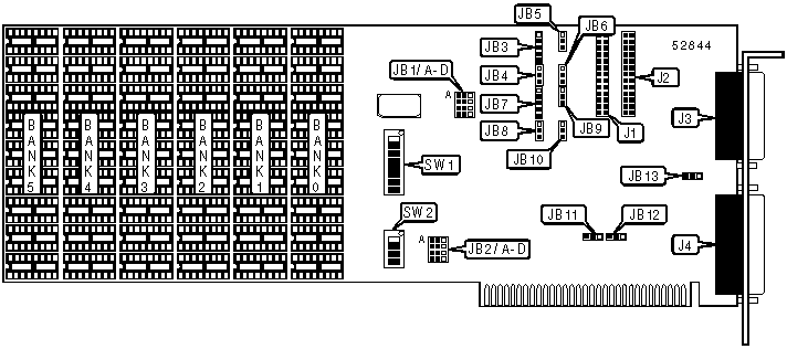
CONNECTIONS | |||
|
Function |
Label |
Function |
Label |
|
Serial port 1 |
J1 |
Game port |
J3 |
|
Serial port 2 |
J2 |
Parallel port |
J4 |
|
USER CONFIGURABLE SETTINGS | |||
|
Setting |
Label |
Position | |
| » |
Factory configured - do not alter |
JB3 |
Pins 2 & 3, 4 & 5 closed |
| » |
Factory configured - do not alter |
JB4 |
Pins 2 & 3 closed |
| » |
Factory configured - do not alter |
JB5 |
Pins 2 & 3 closed |
| » |
Factory configured - do not alter |
JB6 |
Pins 2 & 3 closed |
| » |
Factory configured - do not alter |
JB7 |
Pins 2 & 3, 4 & 5 closed |
| » |
Factory configured - do not alter |
JB8 |
Pins 2 & 3 closed |
| » |
Factory configured - do not alter |
JB9 |
Pins 2 & 3 closed |
| » |
Factory configured - do not alter |
JB10 |
Pins 2 & 3 closed |
| » |
Clock/calendar address set to 377h |
JB11 |
Pins 2 & 3 closed |
|
Clock/calendar address set to 277h |
JB11 |
Pins 1 & 2 closed | |
| » |
Parallel port address set to 378h |
JB12 |
Pins 2 & 3 closed |
|
Parallel port address set to 278h |
JB12 |
Pins 1 & 2 closed | |
| » |
Parallel port is unidirectional |
JB13 |
Pins 2 & 3 closed |
|
Parallel port is bidirectional |
JB13 |
Pins 1 & 2 closed | |
| » |
Game port enabled |
SW1/4 |
On |
|
Game port disabled |
SW1/4 |
Off | |
|
USER CONFIGURABLE SETTINGS (CON’T) | |||
|
Setting |
Label |
Position | |
| » |
Parallel port enabled |
SW1/5 |
On |
|
Parallel port disabled |
SW1/5 |
Off | |
| » |
Clock/calendar enabled |
SW1/6 |
On |
|
Clock/calendar disabled |
SW1/6 |
Off | |
| » |
Serial port 2 enabled |
SW1/7 |
On |
|
Serial port 2 disabled |
SW1/7 |
Off | |
| » |
Serial port 1 enabled |
SW1/8 |
On |
|
Serial port 1 disabled |
SW1/8 |
Off | |
| » |
Parity checking on memory enabled |
SW2/4 |
On |
|
Parity checking on memory disabled |
SW2/4 |
Off | |
|
Note:Jumpers JB3 through JB10 are used for shorting or swapping serial port signals. JB3 through JB6 are for port 1, and JB7 through JB10 are for port 2. Defaults shown are for standard DTE setting. Other configurations are unidentified. | |||
|
STARTING MEMORY ADDRESS SELECTION | |||
|
Setting |
SW1/1 |
SW1/2 |
SW1/3 |
|
0KB |
Off |
Off |
Off |
|
64KB |
On |
Off |
Off |
|
128KB |
Off |
On |
Off |
|
192KB |
On |
On |
Off |
|
256KB |
Off |
Off |
On |
|
320KB |
On |
Off |
On |
|
384KB |
Off |
On |
On |
|
448KB |
On |
On |
On |
|
DRAM CONFIGURATION | ||||
|
Setting |
Bank 0 |
Bank 1 |
Bank 2 |
Bank 3 |
|
0KB |
None |
None |
None |
None |
|
64KB |
(9) 64K x 1 |
None |
None |
None |
|
128KB |
(9) 64K x 1 |
(9) 64K x 1 |
None |
None |
|
192KB |
(9) 64K x 1 |
(9) 64K x 1 |
(9) 64K x 1 |
None |
|
256KB |
(9) 64K x 1 |
(9) 64K x 1 |
(9) 64K x 1 |
(9) 64K x 1 |
|
320KB |
(9) 64K x 1 |
(9) 64K x 1 |
(9) 64K x 1 |
(9) 64K x 1 |
|
384KB |
(9) 64K x 1 |
(9) 64K x 1 |
(9) 64K x 1 |
(9) 64K x 1 |
|
512KB |
(9) 64K x 1 |
(9) 64K x 1 |
(9) 64K x 1 |
(9) 64K x 1 |
|
DRAM CONFIGURATION (CON’T) | ||||
|
Setting |
Bank 4 |
Bank 5 |
Bank 6 |
Bank 7 |
|
0KB |
None |
None |
None |
None |
|
64KB |
None |
None |
None |
None |
|
128KB |
None |
None |
None |
None |
|
192KB |
None |
None |
None |
None |
|
256KB |
None |
None |
None |
None |
|
320KB |
(9) 64K x 1 |
None |
None |
None |
|
384KB |
(9) 64K x 1 |
(9) 64K x 1 |
None |
None |
|
512KB |
(9) 64K x 1 |
(9) 64K x 1 |
(9) 64K x 1 |
(9) 64K x 1 |
|
Note:The locations of banks 6 and 7 are unidentified. | ||||
|
DRAM SWITCH CONFIGURATION | |||
|
Setting |
SW2/1 |
SW2/2 |
SW2/3 |
|
0KB |
Off |
Off |
Off |
|
64KB |
On |
Off |
Off |
|
128KB |
Off |
On |
Off |
|
192KB |
On |
On |
Off |
|
256KB |
Off |
Off |
On |
|
320KB |
On |
Off |
On |
|
384KB |
Off |
On |
On |
|
512KB |
On |
On |
On |
|
SERIAL PORT 1 INTERRUPT SELECTION | |||||
|
Setting |
JB1/A |
JB1/B |
JB1/C |
JB1/D | |
|
IRQ2 |
Pins 1 & 2 closed |
Open |
Open |
Open | |
|
IRQ3 |
Open |
Pins 1 & 2 closed |
Open |
Open | |
| » |
IRQ4 |
Open |
Open |
Pins 1 & 2 closed |
Open |
|
IRQ5 |
Open |
Open |
Open |
Pins 1 & 2 closed | |
|
SERIAL PORT 2 INTERRUPT SELECTION | |||||
|
Setting |
JB1/A |
JB1/B |
JB1/C |
JB1/D | |
|
IRQ2 |
Pins 2 & 3 closed |
Open |
Open |
Open | |
| » |
IRQ3 |
Open |
Pins 2 & 3 closed |
Open |
Open |
|
IRQ4 |
Open |
Open |
Pins 2 & 3 closed |
Open | |
|
IRQ5 |
Open |
Open |
Open |
Pins 2 & 3 closed | |
|
SERIAL PORT 1 ADDRESS SELECTION | |||||
|
Setting |
JB2/A |
JB2/B |
JB2/C |
JB2/D | |
| » |
3F8h (COM1:) |
Open |
Open |
Open |
Pins 1 & 2 closed |
|
2F8h (COM2:) |
Open |
Open |
Pins 1 & 2 closed |
Open | |
|
3E8h (COM3:) |
Open |
Pins 1 & 2 closed |
Open |
Open | |
|
2E8h (COM4:) |
Pins 1 & 2 closed |
Open |
Open |
Open | |
|
SERIAL PORT 2 ADDRESS SELECTION | |||||
|
Setting |
JB2/A |
JB2/B |
JB2/C |
JB2/D | |
|
3F8h (COM1:) |
Open |
Open |
Open |
Pins 2 & 3 closed | |
| » |
2F8h (COM2:) |
Open |
Open |
Pins 2 & 3 closed |
Open |
|
3E8h (COM3:) |
Open |
Pins 2 & 3 closed |
Open |
Open | |
|
2E8h (COM4:) |
Pins 2 & 3 closed |
Open |
Open |
Open | |