CSS LABORATORIES, INC.
PREFERRED 486 GA/VL ESP
|
Processor |
80486SX/80487SX/80486DX/80486DX2/Pentium Overdrive |
|
Processor Speed |
25/33/50(internal)50/66(internal)/66MHz |
|
Chip Set |
OPTI |
|
Max. Onboard DRAM |
32/64MB |
|
Cache |
64/256/512KB |
|
BIOS |
AMI |
|
Dimensions |
330mm x 218mm |
|
I/O Options |
32-bit VESA local bus slots (2) |
|
NPU Options |
None |
|
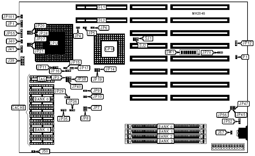
CONNECTIONS | |||
|
Purpose |
Location |
Purpose |
Location |
|
Front panel connector |
J39 |
Power LED & keylock |
JP55 |
|
IDE interface LED |
J40 |
Turbo switch |
JP101 |
|
Turbo LED/reset switch |
J41 |
Video to green connector |
P1 |
|
Speaker |
JP1 |
32-bit VESA Local bus slots |
SL1 & SL2 |
|
USER CONFIGURABLE SETTINGS | |||
|
Function |
Jumper/Switch |
Position | |
|
» |
Green PC password enabled |
J57 |
Open |
|
Green PC password disabled |
J57 |
Closed | |
|
» |
VESA bus clock select CPU speed & 1 clock |
JP7 |
Closed |
|
VESA bus clock select CPU speed |
JP7 |
Open | |
|
» |
Cache burst mode select 2-1-1-1 |
JP9 |
Open |
|
Cache burst mode select 3-2-2-2 |
JP9 |
Closed | |
|
» |
CPU type select DX/DX2/Overdrive |
JP11 |
Pins 2 & 3 closed |
|
CPU type select Overdrive |
JP11 |
Pins 1 & 2 closed | |
|
» |
CPU type select non SX CPU |
JP14 |
Open |
|
CPU type select SX CPU |
JP14 |
Pins 2 & 3 closed | |
|
» |
Video card address select C000h-C7FFh disabled |
JP47 |
Open |
|
Video card address select C000h-C7FFh enabled |
JP47 |
Closed | |
|
» |
Flash BIOS enabled |
JP52 |
Pins 1 & 2 closed |
|
Flash BIOS disabled |
JP52 |
Pins 2 & 3 closed | |
|
» |
Monitor type select color |
JP56 |
Closed |
|
Monitor type select monochrome |
JP56 |
Open | |
|
» |
Keyboard synchronous with CPU |
JP70 |
Pins 2 & 3 closed |
|
Engineer test setting |
JP70 |
Pins 1 & 2 closed | |
|
» |
Factory configured - do not alter. |
SW1/7 |
Off |
|
» |
Factory configured - do not alter |
SW1/8 |
Off |
|
DRAM CONFIGURATION (30PIN) | ||
|
Size |
Bank 0 |
Bank 1 |
|
4MB |
(4) 1M x 9 |
NONE |
|
8MB |
(4) 1M x 9 |
(4) 1M x 9 |
|
16MB |
(4) 4M x 9 |
NONE |
|
20MB |
(4) 1M x 9 |
(4) 4M x 9 |
|
32MB |
(4) 4M x 9 |
(4) 4M x 9 |
|
Note: This board was manufactured with either 8 banks of 30 pin SIMM sockets or 4 banks of 72 pin SIMM sockets. Mainboard drawing depicts 72 pin SIMM sockets. If mainboard has 30 pin SIMM sockets, use the above table. | ||
|
DRAM CONFIGURATION (72 PIN) | ||||
|
Size |
Bank 0 |
Bank 1 |
Bank 2 |
Bank 3 |
|
2MB |
(1) 512K x 36 |
NONE |
NONE |
NONE |
|
4MB |
(1) 512K x 36 |
(1) 512K x 36 |
NONE |
NONE |
|
4MB |
(1) 1M x 36 |
NONE |
NONE |
NONE |
|
6MB |
(1) 512K x 36 |
(1) 1M x 36 |
NONE |
NONE |
|
8MB |
(1) 1M x 36 |
(1) 1M x 36 |
NONE |
NONE |
|
8MB |
(1) 2M x 36 |
NONE |
NONE |
NONE |
|
10MB |
(1) 512K x 36 |
(1) 2M x 36 |
NONE |
NONE |
|
12MB |
(1) 1M x 36 |
(1) 2M x 36 |
NONE |
NONE |
|
12MB |
(1) 512K x 36 |
(1) 512K x 36 |
(1) 2M x 36 |
NONE |
|
14MB |
(1) 512K x 36 |
(1) 1M x 36 |
(1) 2M x 36 |
NONE |
|
16MB |
(1) 2M x 36 |
(1) 2M x 36 |
NONE |
NONE |
|
16MB |
(1) 4M x 36 |
NONE |
NONE |
NONE |
|
16MB |
(1) 1M x 36 |
(1) 1M x 36 |
(1) 2M x 36 |
NONE |
|
18MB |
(1) 512K x 36 |
(1) 2M x 36 |
(1) 2M x 36 |
NONE |
|
20MB |
(1) 512K x 36 |
(1) 512K x 36 |
(1) 2M x 36 |
(1) 2M x 36 |
|
20MB |
(1) 1M x 36 |
(1) 2M x 36 |
(1) 2M x 36 |
NONE |
|
22MB |
(1) 512K x 36 |
(1) 1M x 36 |
(1) 2M x 36 |
(1) 2M x 36 |
|
24MB |
(1) 1M x 36 |
(1) 1M x 36 |
(1) 2M x 36 |
(1) 2M x 36 |
|
24MB |
(1) 2M x 36 |
(1) 2M x 36 |
(1) 2M x 36 |
NONE |
|
24MB |
(1) 1M x 36 |
(1) 1M x 36 |
(1) 4M x 36 |
NONE |
|
26MB |
(1) 512K x 36 |
(1) 2M x 36 |
(1) 2M x 36 |
(1) 2M x 36 |
|
28MB |
(1) 1M x 36 |
(1) 2M x 36 |
(1) 2M x 36 |
(1) 2M x 36 |
|
32MB |
(1) 4M x 36 |
(1) 4M x 36 |
NONE |
NONE |
|
32MB |
(1) 8M x 36 |
NONE |
NONE |
NONE |
|
32MB |
(1) 2M x 36 |
(1) 2M x 36 |
(1) 2M x 36 |
(1) 2M x 36 |
|
32MB |
(1) 2M x 36 |
(1) 2M x 36 |
(1) 4M x 36 |
NONE |
|
40MB |
(1) 1M x 36 |
(1) 1M x 36 |
(1) 4M x 36 |
(1) 4M x 36 |
|
48MB |
(1) 2M x 36 |
(1) 2M x 36 |
(1) 4M x 36 |
(1) 4M x 36 |
|
48MB |
(1) 4M x 36 |
(1) 4M x 36 |
(1) 4M x 36 |
NONE |
|
64MB |
(1) 4M x 36 |
(1) 4M x 36 |
(1) 4M x 36 |
(1) 4M x 36 |
|
64MB |
(1) 4M x 36 |
(1) 4M x 36 |
(1) 8M x 36 |
NONE |
|
Note: This board was manufactured with either 8 banks of 30 pin SIMM sockets or 4 banks of 72 pin SIMM sockets. Mainboard drawing depicts 72 pin SIMM sockets. If mainboard has 72 pin SIMM sockets, use the above table. | ||||
|
CACHE CONFIGURATION | |||
|
Size |
Bank 0 |
Bank 1 |
TAG |
|
64KB |
(4) 8K x 8 |
(4) 8K x 8 |
(1) 8K x 8 |
|
256KB |
(4) 32K x 8 |
(4) 32K x 8 |
(1) 32K x 8 |
|
512KB |
(4) 128K x 8 |
NONE |
(1) 32K x 8 |
|
CACHE JUMPER CONFIGURATION | |||||||||
|
Size |
JP20 |
JP21 |
JP27 |
JP28 |
JP29 |
JP35 |
JP36 |
JP38 |
JP40 |
|
64KB |
1 & 2 |
1 & 2 |
1 & 2 |
1 & 2 |
2 & 3 |
2 & 3 |
2 & 3 |
1 & 2 |
2 & 3 |
|
256KB |
1 & 2 |
2 & 3 |
2 & 3 |
2 & 3 |
2 & 3 |
2 & 3 |
2 & 3 |
1 & 2 |
2 & 3 |
|
512KB |
2 & 3 |
2 & 3 |
2 & 3 |
2 & 3 |
1 & 2 |
1 & 2 |
1 & 2 |
2 & 3 |
1 & 2 |
|
Note: Pins designated should be in the closed position. | |||||||||
|
CPU TYPE CONFIGURATION | |||
|
Type |
JP15 |
JP16 |
JP17 |
|
80486SX |
Open |
Pins 2 & 3 closed |
Open |
|
80486DX |
Closed |
Pins 1 & 2 closed |
Closed |
|
OVERDRIVE/80486SX CONFIGURATION | ||
|
Type |
JP12 | |
| » |
Both sockets enabled |
Open |
|
80486SX disabled |
Pins 1 & 2 closed | |
|
Overdrive disabled |
Pins 2 & 3 closed | |
|
CPU SPEED CONFIGURATION | |||
|
Speed |
JP8 |
JP19 |
JP50 |
|
25MHz |
Closed |
Pins 1 & 2 closed |
N/A |
|
33MHz |
Closed |
Pins 1 & 2 closed |
N/A |
|
50iMHz |
Open |
Pins 2 & 3 closed |
N/A |
|
50MHz |
N/A |
N/A |
Closed |
|
66iMHz |
Open |
Pins 2 & 3 closed |
N/A |
|
66MHz |
N/A |
N/A |
Open |
|
VESA SYSTEM SPEED CONFIGURATION | |
|
CPU speed |
JP4 |
|
< 33MHz |
Open |
|
>= 33MHz |
Closed |
|
VESA WAIT STATE | |||
|
Setting |
JP5 |
JP6 |
JP10 |
|
0 wait states |
Open |
Open |
Open |
|
1 wait state |
Closed |
Closed |
Closed |
|
GREEN PC IRQ DETECTION | ||||||
|
IRQ |
SW1/1 |
SW1/2 |
SW1/3 |
SW1/4 |
SW1/5 |
SW1/6 |
|
IRQ3 |
Off |
Off |
On |
Off |
Off |
Off |
|
IRQ4 |
Off |
Off |
Off |
Off |
On |
Off |
|
IRQ6 |
Off |
Off |
Off |
Off |
Off |
On |
|
IRQ10 |
On |
Off |
Off |
Off |
Off |
Off |
|
IRQ11 |
Off |
On |
Off |
Off |
Off |
Off |
|
IRQ14 |
Off |
Off |
Off |
On |
Off |
Off |
|
IRQ CONFIGURATION | |||
|
IRQ |
SJ1 |
SJ2 | |
| » |
IRQ5 & IRQ7 |
Pins 1 & 2 closed |
Pins 1 & 2 closed |
|
IRQ12 & IRQ15 |
Pins 2 & 3 closed |
Pins 2 & 3 closed | |
|
EXTENDED READY SIGNAL CONFIGURATION | ||
|
CPU Speed |
JP3 |
JP45 |
|
> 33mhz (RDY1) |
Pins 2 & 3 closed |
Closed |
|
< 25mhz (RDY2) |
Pins 1 & 2 closed |
Open |
|
FRONT PANEL PIN OUT CONFIGURATION | |
|
Pin |
Assignment |
|
1 |
Ground |
|
2 |
Power LED |
|
3 |
Hard drive LED |
|
4 |
Not used |
|
5 |
Power |
|
6 |
Ground |
|
7 |
Turbo LED |
|
8 |
Keyboard inhibit |
|
9 |
Power |
|
10 |
Reset switch |