INTEL CORPORATION
TE430VX
|
Processor |
Pentium |
|
Processor Speed |
75/90/100/120/133/150/166/200MHz |
|
Chip Set |
Intel |
|
Video Chip Set |
S3 |
|
Maximum Onboard Memory |
128MB (EDO supported) |
|
Maximum Video Memory |
2MB |
|
Cache |
256/512KB |
|
BIOS |
AMI |
|
Dimensions |
305mm x 244mm |
|
I/O Options |
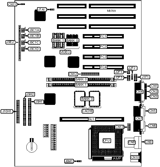
32-bit PCI slots (4), CD-ROM interface, floppy drive interface, green PC connector, IDE interfaces (2), parallel port, PS/2 mouse port, serial ports (2), VESA feature connector, VGA port, cache slot, IR connector, USB connectors (2), modem blaster connector, wave table connector, telephony connector, microphone in connector, line in connector, line out connector, MIDI/game port |
|
NPU Options |
None |
|
CONNECTIONS | |||
|
Purpose |
Location |
Purpose |
Location |
|
Microphone connector |
CN1 |
CD-ROM connector |
J2F2 |
|
Line in connector |
CN2 |
Wave table connector |
J2F3 |
|
Line out connector |
CN3 |
Power on connector |
J9E2 pins 1 & 2 |
|
MIDI/game port |
CN4 |
Green PC connector |
J9E2 pins 3 & 4 |
|
VGA port |
CN5 |
IR connector |
J9E2 pins 6 - 11 |
|
Serial port 1 |
CN6 |
IDE interface LED |
J9E2 pins 13 - 16 |
|
Parallel port |
CN7 |
Green PC LED |
J9E2 pins 18 - 21 |
|
USB connector |
CN8 |
Reset switch |
J9E2 pins 22 & 23 |
|
USB connector |
CN9 |
Speaker |
J9E2 pins 24 - 27 |
|
PS/2 mouse port |
CN10 |
IDE interface 1 |
J9H1 |
|
Chassis fan power |
CN11 |
IDE interface 2 |
J9H2 |
|
VESA feature connector |
CN12 |
Floppy drive interface |
J10H1 |
|
Serial port 2 |
CN13 |
32-bit PCI slots |
PC1 - PC4 |
|
Modem blaster connector |
J1F1 |
Cache slot |
SL1 |
|
Telephony connector |
J2F1 | ||
|
USER CONFIGURABLE SETTINGS | |||
|
Function |
Label |
Position | |
|
» |
Flash BIOS normal operation |
J7A1 |
Pins 1 & 2 closed |
|
Flash BIOS recovery mode |
J7A1 |
Pins 2 & 3 closed | |
|
» |
Password normal operation |
J9C1A |
Pins 1 & 2 closed |
|
Password clear |
J9C1A |
Pins 2 & 3 closed | |
|
» |
CMOS memory normal operation |
J9C1A |
Pins 4 & 5 closed |
|
CMOS memory clear |
J9C1A |
Pins 5 & 6 closed | |
|
» |
Setup access enabled |
J9C1B |
Pins 1 & 2 closed |
|
Setup access disabled |
J9C1B |
Pins 2 & 3 closed | |
|
» |
Factory configured - do not alter |
J9C1B |
Open |
|
DRAM CONFIGURATION (SDRAM) | ||
|
Size |
Bank 0 |
Bank 1 |
|
8MB |
(1) 1M x 64 |
None |
|
16MB |
(1) 2M x 64 |
None |
|
32MB |
(1) 4M x 64 |
None |
|
16MB |
(1) 1M x 64 |
(1) 1M x 64 |
|
24MB |
(1) 2M x 64 |
(1) 1M x 64 |
|
40MB |
(1) 4M x 64 |
(1) 1M x 64 |
|
32MB |
(1) 2M x 64 |
(1) 2M x 64 |
|
48MB |
(1) 4M x 64 |
(1) 2M x 64 |
|
64MB |
(1) 4M x 64 |
(1) 4M x 64 |
|
DRAM CONFIGURATION (DIMM EDO) | ||
|
Size |
Bank 0 |
Bank 1 |
|
8MB |
(1) 1M x 64 |
None |
|
16MB |
(1) 2M x 64 |
None |
|
16MB |
(1) 1M x 64 |
(1) 1M x 64 |
|
24MB |
(1) 2M x 64 |
(1) 1M x 64 |
|
32MB |
(1) 4M x 64 |
None |
|
32MB |
(1) 2M x 64 |
(1) 2M x 64 |
|
40MB |
(1) 4M x 64 |
(1) 1M x 64 |
|
48MB |
(1) 4M x 64 |
(1) 2M x 64 |
|
64MB |
(1) 8M x 64 |
None |
|
64MB |
(1) 4M x 64 |
(1) 4M x 64 |
|
72MB |
(1) 8M x 64 |
(1) 1M x 64 |
|
80MB |
(1) 8M x 64 |
(1) 2M x 64 |
|
96MB |
(1) 8M x 64 |
(1) 4M x 64 |
|
128MB |
(1) 8M x 64 |
(1) 8M x 64 |
|
CACHE CONFIGURATION | ||
|
Size |
Bank 0 |
SL1 |
|
256KB |
(2) 32K x 32 |
Not installed |
|
512KB |
(2) 32K x 32 |
256KB module installed |
|
Note: The location of the TAG chip is unidentified. | ||
|
VIDEO MEMORY CONFIGURATION | ||
|
Size |
Bank 0 |
Bank 1 |
|
1MB |
1MB |
None |
|
2MB |
1MB |
(2) 256K x 16 |
|
Note: Bank 0 is factory installed and is not configurable. | ||
|
CPU SPEED SELECTION | ||||
|
CPU speed |
Clock speed |
Multiplier |
J9C1C |
J9C1D |
|
75MHz |
50MHz |
1.5x |
2 & 3, 5 & 6 |
1 & 2, 4 & 5 |
|
90MHz |
60MHz |
1.5x |
2 & 3, 4 & 5 |
1 & 2, 4 & 5 |
|
100MHz |
66MHz |
1.5x |
1 & 2, 5 & 6 |
1 & 2, 4 & 5 |
|
120MHz |
60MHz |
2x |
2 & 3, 4 & 5 |
2 & 3, 4 & 5 |
|
133MHz |
66MHz |
2x |
1 & 2, 5 & 6 |
2 & 3, 4 & 5 |
|
150MHz |
60MHz |
2.5x |
2 & 3, 4 & 5 |
1 & 2, 5 & 6 |
|
166MHz |
66MHz |
2.5x |
1 & 2, 5 & 6 |
1 & 2, 5 & 6 |
|
200MHz |
66MHz |
3x |
1 & 2, 5 & 6 |
2 & 3, 5 & 6 |
|
Note: Pins designated should be in the closed position. | ||||
|
CPU TYPE SELECTION | |
|
Type |
J6M1 |
|
VR |
Pins 2 & 3 closed |
|
VRE |
Pins 1 & 2 closed |