FREE COMPUTER TECHNOLOGY, INC.
486F39X, 486VL VIII
|
Processor |
CX486S/80486SX/80486SX2/CX486DX/80486DX/CX486DX2/80486DX2/ 80486DX4/Pentium Overdrive |
|
Processor Speed |
25/33/40/50(internal)/50/66(internal)MHz |
|
Chip Set |
OPTI |
|
Max. Onboard DRAM |
64MB |
|
Cache |
128/256/512KB |
|
BIOS |
Award |
|
Dimensions |
330mm x 218mm |
|
I/O Options |
32-bit VESA local bus slots (3), green PC connector |
|
NPU Options |
None |
|
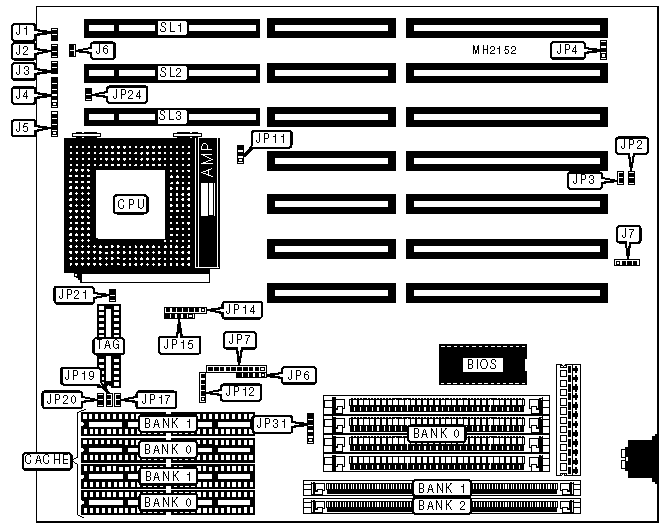
CONNECTIONS | |||
|
Purpose |
Location |
Purpose |
Location |
|
Turbo switch |
J1 |
Break switch |
J6 |
|
Turbo LED |
J2 |
External battery |
J7 |
|
Reset switch |
J3 |
Green PC connector |
JP2 |
|
Power LED & keylock |
J4 |
Green PC connector |
JP3 |
|
Speaker |
J5 |
32-bit VESA Local bus slots |
SL1 - SL3 |
|
USER CONFIGURABLE SETTINGS | |||
|
Function |
Jumper |
Position | |
|
» |
CMOS memory normal operation |
JP4 |
pins 2 & 3 closed |
|
CMOS memory clear |
JP4 |
pins 1 & 2 closed | |
|
DRAM CONFIGURATION (GROUP 1) | |||
|
Size |
Bank 0 |
Bank 1 |
Bank 2 |
|
1MB |
(4) 256Kx 9 |
NONE |
NONE |
|
2MB |
(4) 256K x 9 |
(1) 256K x 36 |
NONE |
|
4MB |
(4) 256K x 9 |
(1) 256K x 36 |
(1) 512K x 36 |
|
4MB |
(4) 1M x 9 |
NONE |
NONE |
|
5MB |
(4) 256K x 9 |
(1) 1M x 36 |
NONE |
|
6MB |
(4) 256K x 9 |
(1) 256K x 36 |
(1) 1M x 36 |
|
8MB |
(4) 1M x 9 |
(1) 1M x 36 |
NONE |
|
10MB |
(4) 256K x 9 |
(1) 256K x 36 |
(1) 2M x 36 |
|
12MB |
(4) 1M x 9 |
(1) 1M x 36 |
(1) 1M x 36 |
|
16MB |
(4) 4M x 9 |
NONE |
NONE |
|
16MB |
(4) 1M x 9 |
(1) 1M x 36 |
(1) 2M x 36 |
|
17MB |
(4) 256K x 9 |
(1) 4M x 36 |
NONE |
|
18MB |
(4) 256K x 9 |
(1) 256K x 36 |
(1) 4M x 36 |
|
20MB |
(4) 1M x 9 |
(1) 4M x 36 |
NONE |
|
24MB |
(4) 1M x 9 |
(1) 1M x 36 |
(1) 4M x 36 |
|
32MB |
(4) 4M x 9 |
(1) 4M x 36 |
NONE |
|
36MB |
(4) 1M x 9 |
(1) 4M x 36 |
(1) 4M x 36 |
|
40MB |
(4) 1M x 9 |
(1) 1M x 36 |
(1) 8M x 36 |
|
48MB |
(4) 4M x 9 |
(1) 4M x 36 |
(1) 4M x 36 |
|
64MB |
(4) 4M x 9 |
(1) 4M x 36 |
(1) 8M x 36 |
|
DRAM CONFIGURATION (GROUP 2) | |||
|
Size |
Bank 0 |
Bank 1 |
Bank 2 |
|
1MB |
NONE |
(1) 256K x 36 |
NONE |
|
2MB |
NONE |
(1) 256K x 36 |
(1) 256K x 36 |
|
4MB |
NONE |
(1) 1M x 36 |
NONE |
|
5MB |
NONE |
(1) 256K x 36 |
(1) 1M x 36 |
|
8MB |
NONE |
(1) 1M x 36 |
(1) 1M x 36 |
|
16MB |
NONE |
(1) 4M x 36 |
NONE |
|
17MB |
NONE |
(1) 256K x 36 |
(1) 4M x 36 |
|
20MB |
NONE |
(1) 1M x 36 |
(1) 4M x 36 |
|
32MB |
NONE |
(1) 4M x 36 |
(1) 4M x 36 |
|
DRAM CONFIGURATION (GROUP 3) | |||
|
Size |
Bank 0 |
Bank 1 |
Bank 2 |
|
2MB |
NONE |
(1) 512K x 36 |
NONE |
|
4MB |
NONE |
(1) 512K x 36 |
(1) 512K x 36 |
|
6MB |
NONE |
(1) 512K x 36 |
(1) 1M x 36 |
|
8MB |
NONE |
(1) 2M x 36 |
NONE |
|
10MB |
NONE |
(1) 512K x 36 |
(1) 2M x 36 |
|
12MB |
NONE |
(1) 2M x 36 |
(1) 1M x 36 |
|
16MB |
NONE |
(1) 2M x 36 |
(1) 2M x 36 |
|
18MB |
NONE |
(1) 512K x 36 |
(1) 4M x 36 |
|
24MB |
NONE |
(1) 2M x 36 |
(1) 4M x 36 |
|
32MB |
NONE |
(1) 8M x 36 |
NONE |
|
40MB |
NONE |
(1) 2M x 36 |
(1) 8M x 36 |
|
48MB |
NONE |
(1) 8M x 36 |
(1) 4M x 36 |
|
64MB |
NONE |
(1) 8M x 36 |
(1) 8M x 36 |
|
DRAM JUMPER CONFIGURATION | |
|
Group |
JP31 |
|
Group 1 |
pins 2 & 3, 4 & 5 closed |
|
Group 2 |
pins 1 & 2, 3 & 4 closed |
|
Group 3 |
pins 1 & 2, 4 & 5 closed |
|
CACHE CONFIGURATION | |||
|
Size |
Bank 0 |
Bank 1 |
TAG |
|
128KB |
(4) 32K x 8 |
NONE |
(1) 8K x 8 |
|
256KB |
(4) 32K x 8 |
(4) 32K x 8 |
(1) 16K x 8 or (1) 32K x 8 |
|
256KB |
(4) 64K x 8 |
NONE |
(1) 16K x 8 or (1) 32K x 8 |
|
512KB |
(4) 64K x 8 |
(4) 64K x 8 |
(1) 32K x 8 |
|
512KB |
(4) 128K x 8 |
NONE |
(1) 32K x 8 |
|
CACHE JUMPER CONFIGURATION | ||
|
Size |
JP12 |
JP21 |
|
128KB |
pins 1 & 2 closed |
Open |
|
256KB |
pins 2 & 3 closed |
Open |
|
256KB |
pins 1 & 2, 3 & 4 closed |
Open |
|
512KB |
pins 2 & 3, 4 & 5 closed |
Closed |
|
512KB |
pins 1 & 2, 3 & 4 closed |
Closed |
|
CPU TYPE CONFIGURATION | ||
|
Type |
JP6 |
JP7 |
|
CX486S |
1 & 2, 3 & 4 |
2 & 3, 4 & 5, 7 & 8, 9 & 10 |
|
80486SX/SX2 |
2 & 3, 4 & 5 |
1 & 2, 3 & 4, 6 & 7, 8 & 9 |
|
CX486DX |
1 & 2, 3 & 4 |
2 & 3, 4 & 5, 7 & 8, 9 & 10 |
|
CX486DX2 |
1 & 2, 3 & 4 |
2 & 3, 4 & 5, 7 & 8, 9 & 10 |
|
80486DX/DX2 |
2 & 3, 4 & 5 |
1 & 2, 3 & 4, 6 & 7, 8 & 9 |
|
80486DX4 (2x) |
2 & 3, 4 & 5 |
1 & 2, 3 & 4, 6 & 7, 8 & 9 |
|
80486DX4 (2.5x) |
2 & 3, 4 & 5 |
1 & 2, 3 & 4, 6 & 7, 8 & 9 |
|
80486DX4 (3x) |
2 & 3, 4 & 5 |
1 & 2, 3 & 4, 6 & 7, 8 & 9 |
|
Overdrive |
2 & 3, 4 & 5 |
1 & 2, 3 & 4, 6 & 7, 8 & 9 |
|
Pentium Overdrive |
1 & 2, 4 & 5 |
1 & 2, 3 & 4, 6 & 7, 8 & 9 |
|
Note: Pins designated should be in the closed position. | ||
|
CPU TYPE CONFIGURATION (CON’T) | |||
|
Type |
JP11 |
JP14 |
JP15 |
|
CX486S |
Open |
2 & 3, 5 & 6 |
3 & 4 |
|
80486SX/SX2 |
Open |
2 & 3, 4 & 5, 6 & 7 |
3 & 4 |
|
CX486DX |
Open |
3 & 4 |
1 & 2, 5 & 6 |
|
CX486DX2 |
Open |
1 & 2, 5 & 6 |
1 & 2, 3 & 4 |
|
80486DX/DX2 |
Open |
1 & 2, 4 & 5, 6 & 7 |
3 & 4 |
|
80486DX4 (2x) |
2 & 3 |
1 & 2, 4 & 5, 6 & 7 |
3 & 4 |
|
80486DX4 (2.5x) |
1 & 2 |
1 & 2, 4 & 5, 6 & 7 |
3 & 4 |
|
80486DX4 (3x) |
Open |
1 & 2, 4 & 5, 6 & 7 |
3 & 4 |
|
Overdrive |
Open |
1 & 2, 4 & 5, 6 & 7 |
3 & 4 |
|
Pentium Overdrive |
Open |
1 & 2, 4 & 5, 6 & 7 |
4 & 5 |
|
Note: Pins designated should be in the closed position. | |||
|
CPU SPEED CONFIGURATION | |||
|
Speed |
JP17 |
JP19 |
JP20 |
|
25MHz |
Closed |
Open |
Closed |
|
33MHz |
Closed |
Closed |
Open |
|
40MHz |
Open |
Open |
Closed |
|
50iMHz |
Closed |
Open |
Closed |
|
50MHz |
Open |
Closed |
Open |
|
66iMHz |
Closed |
Closed |
Open |
|
BUS SPEED CONFIGURATION | |
|
CPU speed |
JP24 |
|
<=33MHz |
Open |
|
>33MHz |
Closed |