MITSUMI ELECTRONICS CORPORATION
EXTERNAL CD-ROM INTERFACE CARD (VER. 1)
|
Card Type |
CD-ROM interface card |
|
Chip Set |
Unidentified |
|
Maximum Onboard Memory |
None |
|
I/O Options |
None |
|
Data Bus |
8-bit ISA |
|
Floppy drives supported |
None |
|
CONNECTIONS | |
|
Function |
Label |
|
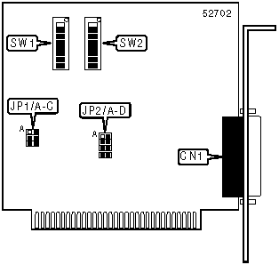
CD-ROM interface connector |
CN1 |
|
USER CONFIGURABLE SETTINGS | |||
|
Function |
Label |
Position | |
| » |
Factory configured - do not alter |
SW2/1 |
On |
| » |
Factory configured - do not alter |
SW2/2 |
On |
| » |
Factory configured - do not alter |
SW2/3 |
On |
| » |
Factory configured - do not alter |
SW2/4 |
Off |
| » |
Factory configured - do not alter |
SW2/5 |
Off |
| » |
Factory configured - do not alter |
SW2/6 |
Off |
| » |
Factory configured - do not alter |
SW2/7 |
Off |
| » |
Factory configured - do not alter |
SW2/8 |
Off |
|
DMA CHANNEL SELECTION | |||||
|
Channel |
JP2/A |
JP2/B |
JP2/C |
JP2/D | |
|
1 |
Closed |
Closed |
Open |
Open | |
| » |
3 |
Open |
Open |
Closed |
Closed |
|
BASE I/O ADDRESS SELECTION | |||||||||
|
Setting |
SW1/1 |
SW1/2 |
SW1/3 |
SW1/4 |
SW1/5 |
SW1/6 |
SW1/7 |
SW1/8 | |
|
0h |
On |
On |
On |
On |
On |
On |
On |
On | |
|
4h |
Off |
On |
On |
On |
On |
On |
On |
On | |
|
8h |
On |
Off |
On |
On |
On |
On |
On |
On | |
|
Ch |
Off |
Off |
On |
On |
On |
On |
On |
On | |
|
10h |
On |
On |
Off |
On |
On |
On |
On |
On | |
| » |
300h |
On |
On |
On |
On |
On |
On |
Off |
Off |
|
3ECh |
Off |
Off |
On |
Off |
Off |
Off |
Off |
Off | |
|
3F0h |
On |
On |
Off |
Off |
Off |
Off |
Off |
Off | |
|
3F4h |
Off |
On |
Off |
Off |
Off |
Off |
Off |
Off | |
|
3F8h |
On |
Off |
Off |
Off |
Off |
Off |
Off |
Off | |
|
3FCh |
Off |
Off |
Off |
Off |
Off |
Off |
Off |
Off | |
|
Note:A total of 256 base address settings are available. The switches are a binary representation of the decimal memory addresses. SW1/8 is the Most Significant Bit and switch SW1/1 is the Least Significant Bit. The switches have the following decimal values: SW1/8=512, SW1/7=256, SW1/6=128, SW1/5=64, SW1/4=32, SW1/3=16, SW1/2=8, SW1/1=4. Turn off the switches and add the values of the switches to obtain the correct memory address. (Off=1, On=0) | |||||||||
|
INTERRUPT SELECTION | ||||
|
IRQ |
JP1/A |
JP1/B |
JP1/C | |
|
IRQ2 |
Closed |
Open |
Open | |
| » |
IRQ3 |
Open |
Closed |
Open |
|
IRQ5 |
Open |
Open |
Closed | |