QUATECH, INC.
DDS-100
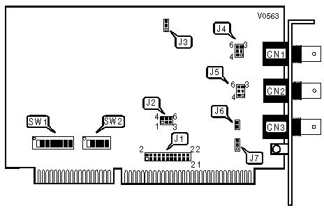
|
Card Type |
Waveform Synthesizer |
|
Chipset/Controller |
Unidentified |
|
I/O Options |
Trigger/gate signal inputs |
|
Maximum DRAM |
N/A |
|
CONNECTIONS | |||
|
Purpose |
Location |
Purpose |
Location |
|
Sine wave output |
CN1 |
Trigger/gate input |
CN3 |
|
TTL square wave/time mark output |
CN2 | ||
|
INTERRUPT SELECT | ||
|
IRQ |
J1 | |
| » |
IRQ5 |
Pins 7 & 8 closed |
|
IRQ2 |
Pins 1 & 2 closed | |
|
IRQ3 |
Pins 3 & 4 closed | |
|
IRQ4 |
Pins 5 & 6 closed | |
|
IRQ6 |
Pins 9 & 10 closed | |
|
IRQ7 |
Pins 11 & 12 closed | |
|
IRQ10 |
Pins 13 & 14 closed | |
|
IRQ11 |
Pins 15 & 16 closed | |
|
IRQ12 |
Pins 17 & 18 closed | |
|
IRQ14 |
Pins 19 & 20 closed | |
|
IRQ15 |
Pins 21 & 22 closed | |
|
Disabled |
All pins open | |
|
8254 CLOCK CONFIGURATION | |
|
Setting |
J2 |
|
10Mhz timer |
Pins 1 & 2, 4 & 5 closed |
|
Cycle counter |
Pins 2 & 3, 5 & 6 closed |
|
8254 CLOCK OUTPUT SPEED | |
|
Output |
J7 |
|
Direct |
Pins 1 & 2 closed |
|
Output/2 |
Pins 2 & 3 closed |
|
Note: Clock input can not exceed 10Mhz. | |
|
SINE WAVE OUTPUT AMPLITUDE | |
|
Setting |
J3 |
|
+ 5V |
Pins 1 & 2 closed |
|
+ 1V |
Pins 2 & 3 closed |
|
SINE WAVE OUTPUT IMPEDANCE | |
|
Output |
J4 |
|
50ohm |
Pins 1 & 2, 4 & 5 closed |
|
75ohm |
Pins 1 & 2, 5 & 6 closed |
|
100ohm |
Pins 1 & 2 closed |
|
Unfiltered |
Pins 2 & 3, 5 & 6 closed |
|
CN2 OUTPUT OPTIONS | |
|
Setting |
J5 |
|
TTL output |
Pins 3 & 6 closed |
|
Clock output |
Pins 2 & 5 closed |
|
Time mark output |
Pins 1 & 4 closed |
|
CN3 INPUT OPTIONS | |
|
Setting |
J6 |
|
External trigger input |
closed |
|
Gate signal input |
open |
|
I/O ADDRESS CONFIGURATION | |||
|
Address |
SW1 |
SW2 | |
| » |
300h |
1, 2, 3, 4, 5 & 6 on |
1, 2, 3, 4 & 5 on |
|
240h |
1, 2, 3, 4, 5, 6 & 8 on |
1, 3, 4 & 5 on | |
|
6FC8h |
1 & 4 on |
3 & 4 on | |
|
Note: The address range for the DDS-100 is from 0 to FFFFh. The switches are a binary representation of the addresses. When a switch is off, the corresponding bit is set to 1 and has the following decimal value: SW1/1=8, SW1/2=4, SW1/3=2, SW1/4=1, SW1/5=8, SW1/6=4, SW1/7=2, SW1/8=1, SW2/1=8, SW2/2=4, SW2/3=2, SW2/4=1, SW2/5=8. The DDS-100 requires eight consecutive address locations. | |||