ACTION INSTRUMENTS
FF486SX/FF486DX
|
Processor |
80486SX/80487SX/80486DX/80486DX2 |
|
Processor Speed |
16/20/25/33/50(internal)/50/66(internal)MHz |
|
Chip Set |
ACC Micro |
|
Max. onboard DRAM |
32MB |
|
SRAM Cache |
None |
|
BIOS |
Phoenix |
|
Dimensions |
337mm x 132mm |
|
I/O Options |
Floppy drive interface, IDE interface, parallel port, serial port (2), VGA port |
|
NPU Options |
None |
|
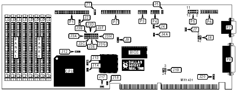
CONNECTIONS | |||
|
Purpose |
Location |
Purpose |
Location |
|
Turbo LED |
J5 |
Serial Port (COM2) |
P4 |
|
IDE interface |
P1 |
LCD panel connector |
P6 |
|
Floppy drive interface |
P2 |
VGA port |
P7 |
|
Serial Port (COM1) |
P3 |
Parallel port |
P8 |
|
PIN OUT CONFIGURATION P5 | |
|
Function |
Pin |
|
Power good signal detect from board |
1 |
|
Keyboard ground |
2 |
|
+ Keyboard clock |
3 |
|
+ 5Vdc |
4 |
|
+ Keyboard data |
5 |
|
Ground |
6 |
|
Reset switch |
7 |
|
Keyboard inhibit switch |
8 |
|
Speaker |
9 & 10 |
|
Not used |
11 & 12 |
|
USER CONFIGURABLE SETTINGS | |||
|
Function |
Jumper |
Position | |
| » |
IDE LED select LED with series resistor (all action instruments. chassis) |
J1 |
pins 1 & 2 |
|
IDE LED select LED only |
J1 |
pins 2 & 3 | |
| » |
IDE interface enabled |
J2 |
pins 2 & 3 |
|
IDE interface disabled |
J2 |
pins 1 & 2 | |
| » |
Floppy drive interface select normal |
J3A |
pins 2 & 3 |
|
Floppy drive interface select encoded |
J3A |
pins 1 & 2 | |
| » |
Floppy drive interface enabled |
J3B |
pins 2 & 3 |
|
Floppy drive interface disabled |
J3B |
pins 1 & 2 | |
| » |
J3A - J3G jumpers enabled |
J3H |
pins 1 & 2 |
|
J3A - J3G jumpers disabled (All J3 settings go to default) |
J3H |
pins 2 & 3 | |
| » |
Watch Dog timer delay 1.2 second |
J4 |
pins 1 & 2 |
|
Watch Dog timer delay 150ms delay |
J4 |
pins 2 & 3 | |
|
Watch Dog timer delay 600ms delay |
J4 |
Open | |
| » |
Watch Dog timer enabled |
J4A |
pins 1 & 2 |
|
Watch Dog timer disabled |
J4A |
pins 2 & 3 | |
| » |
Factory configured - do not alter |
J6 |
Open |
| » |
Monitor type select color |
J7 |
Closed |
|
Monitor type select monochrome |
J7 |
Open | |
| » |
Parallel port select uni-directional (printer) |
J9 |
pins 2 & 3 |
|
Parallel port select bi-directional |
J9 |
pins 1 & 2 | |
| » |
Bus cycle lock enabled |
J14 |
Closed |
|
Bus cycle lock disabled |
J14 |
Open | |
| » |
Last cycle burst enabled |
J17 |
Closed |
|
Last cycle burst disabled |
J17 |
Open | |
| » |
Factory configured - do not alter |
J18 |
Closed |
| » |
IRQ select Internal CRT interrupt |
J20 |
pins 1 & 2 |
|
IRQ select AT bus |
J20 |
pins 2 & 3 | |
|
Note:Pins designated should be in the closed position. | |||
|
DRAM CONFIGURATION | ||
|
Size |
Bank 0 |
Bank 1 |
|
1MB |
(4) 256K x 9 |
NONE |
|
2MB |
(4) 256K x 9 |
(4) 256K x 9 |
|
4MB |
(4) 1M x 9 |
NONE |
|
8MB |
(4) 1M x 9 |
(4) 1M x 9 |
|
16MB |
(4) 4M x 9 |
NONE |
|
20MB |
(4) 1M x 9 |
(4) 4M x 9 |
|
32MB |
(4) 4M x 9 |
(4) 4M x 9 |
|
FLASH MEMORY CONFIGURATION | ||
|
Address |
J19/pins 1 & 2 |
J19/pins 3 & 4 |
|
C0000-C7FFF |
Open |
Open |
|
C8000-CFFFF |
Open |
Closed |
|
D0000-D7FFF |
Closed |
Open |
|
D8000-DFFFF |
Closed |
Closed |
|
SERIAL PORT CONFIGURATION | ||||
|
UART 1/P3 |
UART 2/P4 |
J3C |
J3D |
J3E |
|
COM1 |
COM2 |
pins 2 & 3 |
pins 2 & 3 |
pins 2 & 3 |
|
Disable |
COM2 |
pins 2 & 3 |
pins 2 & 3 |
pins 1 & 2 |
|
COM1 |
Disable |
pins 2 & 3 |
pins 1 & 2 |
pins 2 & 3 |
|
Disable |
Disable |
pins 2 & 3 |
pins 1 & 2 |
pins 1 & 2 |
|
COM2 |
COM1 |
pins 1 & 2 |
pins 2 & 3 |
pins 2 & 3 |
|
Disable |
COM1 |
pins 1 & 2 |
pins 2 & 3 |
pins 1 & 2 |
|
COM2 |
Disable |
pins 1 & 2 |
pins 1 & 2 |
pins 2 & 3 |
|
Disable |
Disable |
pins 1 & 2 |
pins 1 & 2 |
pins 1 & 2 |
|
Note:Pins designated should be in the closed position. | ||||
|
PARALLEL PORT CONFIGURATION | ||||
|
LPT |
ADDRESS |
J3F |
J3G | |
| » |
LPT1 |
378h |
pins 2 & 3 closed |
pins 2 & 3 closed |
|
LPT2 |
278h |
pins 1 & 2 closed |
pins 2 & 3 closed | |
|
LPT3 |
3BCh |
pins 2 & 3 closed |
pins 1 & 2 closed | |
|
Disabled |
N/A |
pins 1 & 2 closed |
pins 1 & 2 closed | |
|
LCD PANEL TYPE/PLASMA PANEL | ||
|
LCD TYPE |
J8/pins 1 & 2 |
J8/pins 3 & 4 |
|
0 |
Open |
Open |
|
1 |
Open |
Closed |
|
2 |
Closed |
Open |
|
3 |
Closed |
Closed |
|
CPU TYPE CONFIGURATION | ||
|
CPU Type |
J12 |
J13 |
|
80486SX |
pins 2 & 3 closed |
pins 2 & 3 closed |
|
80487SX |
pins 1 & 2, 3 & 4 closed |
pins 3 & 4 closed |
|
80486DX |
pins 1 & 2, 3 & 4 closed |
pins 3 & 4 closed |
|
80486DX2 |
pins 1 & 2, 3 & 4 closed |
pins 3 & 4 closed |