LASER COMPUTER, INC.
LASER 486 MODULAR EISA
|
Processor |
80486SX/80487SX/80486DX/80486DX2 |
|
Processor Speed |
16/20/25/33/50(internal)/66(internal)MHz |
|
Chip Set |
Unidentified |
|
Max. Onboard DRAM |
96MB (with two memory cards installed) |
|
Cache |
64/128KB |
|
BIOS |
Unidentified |
|
Dimensions |
330mm x 220mm |
|
I/O Options |
External memory cards (2), external CPU card, PS/2 mouse port |
|
NPU Options |
4167 |

|
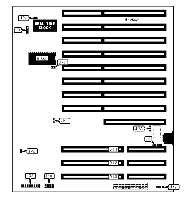
CONNECTIONS | |||
|
Purpose |
Location |
Purpose |
Location |
|
PS/2 mouse connector |
J7 |
Diagnostic connector |
J32 |
|
Speaker |
J9 |
External memory cards |
SL1 & SL2 |
|
Front panel connector |
J10 |
External CPU card |
SL3 |
|
External battery |
J12 | ||
|
USER CONFIGURABLE SETTINGS | |||
|
Function |
Jumper |
Position | |
|
» |
EISA bus controller speed select 25MHz |
JP1 |
Closed |
|
EISA bus controller speed select 33MHz |
JP1 |
Open | |
|
» |
BIOS type select 27512 |
JP2 |
Closed |
|
BIOS type select 27010 |
JP2 |
Open | |
|
» |
Battery type select internal |
JP3 |
pins 2 & 3 closed |
|
Battery type select external |
JP3 |
pins 1 & 2 closed | |
|
» |
Real time clock select MC146818A |
JP4 |
Closed |
|
Real time clock select MC146818 or HD146818 |
JP4 |
Open | |
|
» |
Parity check enabled |
JP5 |
Closed |
|
Parity check disabled |
JP5 |
Open | |

|
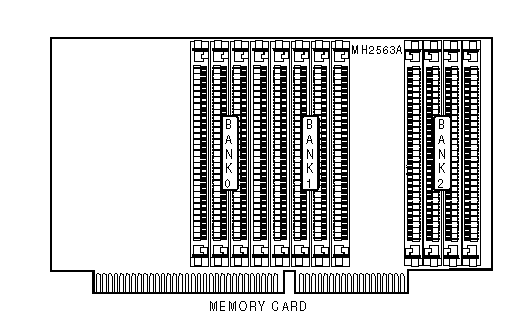
DRAM CONFIGURATION | |||
|
Size |
Bank 0 |
Bank 1 |
Bank 2 |
|
1MB |
(4) 256K x 9 |
NONE |
NONE |
|
2MB |
(4) 256K x 9 |
(4) 256K x 9 |
NONE |
|
3MB |
(4) 256K x 9 |
(4) 256K x 9 |
(4) 256K x 9 |
|
4MB |
(4) 1M x 9 |
NONE |
NONE |
|
5MB |
(4) 256K x 9 |
(4) 1M x 9 |
NONE |
|
8MB |
(4) 1M x 9 |
(4) 1M x 9 |
NONE |
|
9MB |
(4) 256K x 9 |
(4) 1M x 9 |
(4) 1M x 9 |
|
12MB |
(4) 1M x 9 |
(4) 1M x 9 |
(4) 1M x 9 |
|
16MB |
(4) 4M x 9 |
NONE |
NONE |
|
16MB |
(4) 4M x 9 |
NONE |
NONE |
|
17MB |
(4) 256K x 9 |
(4) 4M x 9 |
NONE |
|
20MB |
(4) 1M x 9 |
(4) 4M x 9 |
NONE |
|
20MB |
(4) 4M x 9 |
(4) 1M x 9 |
NONE |
|
24MB |
(4) 4M x 9 |
(4) 1M x 9 |
(4) 1M x 9 |
|
32MB |
(4) 4M x 9 |
(4) 4M x 9 |
NONE |
|
DRAM CONFIGURATION (CON’T) | |||
|
Size |
Bank 0 |
Bank 1 |
Bank 2 |
|
33MB |
(4) 256K x 9 |
(4) 4M x 9 |
(4) 4M x 9 |
|
36MB |
(4) 1M x 9 |
(4) 4M x 9 |
(4) 4M x 9 |
|
48MB |
(4) 4M x 9 |
(4) 4M x 9 |
(4) 4M x 9 |
|
Note: In order to have 96MB, use two memory cards. | |||

|
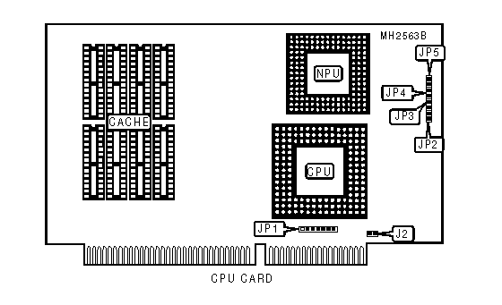
CONNECTIONS | |
|
Purpose |
Location |
|
Chassis fan power |
J2 |
|
USER CONFIGURABLE SETTINGS | |||
|
Function |
Jumper |
Position | |
|
» |
Factory configured - do not alter |
JP2 |
N/A |
|
CACHE CONFIGURATION | ||
|
Size |
Bank 0 |
Bank 1 |
|
64KB |
(4) 8K x 8 |
(4) 8K x 8 |
|
128KB |
(4) 32K x 8 |
NONE |
|
Note: The orientation of the cache banks are unidentified. | ||
|
CPU TYPE CONFIGURATION | |
|
Type |
JP1 |
|
80486SX |
pins 5 & 6 closed |
|
80487SX |
pins 2 & 3, 4 & 5, 6 & 7 closed |
|
80486DX |
pins 1 & 2, 4 & 5, 6 & 7 closed |
|
80486DX2 |
pins 1 & 2, 4 & 5, 6 & 7 closed |
|
CPU SPEED CONFIGURATION | |||
|
Speed |
JP3 |
JP4 |
JP5 |
|
16MHz |
Closed |
Closed |
Closed |
|
20MHz |
Closed |
Closed |
Open |
|
25MHz |
Closed |
Open |
Closed |
|
33MHz |
Closed |
Open |
Open |
|
50iMHz |
Closed |
Open |
Closed |
|
66iMHz |
Closed |
Open |
Open |