TMC RESEARCH CORPORATION
PET48PN
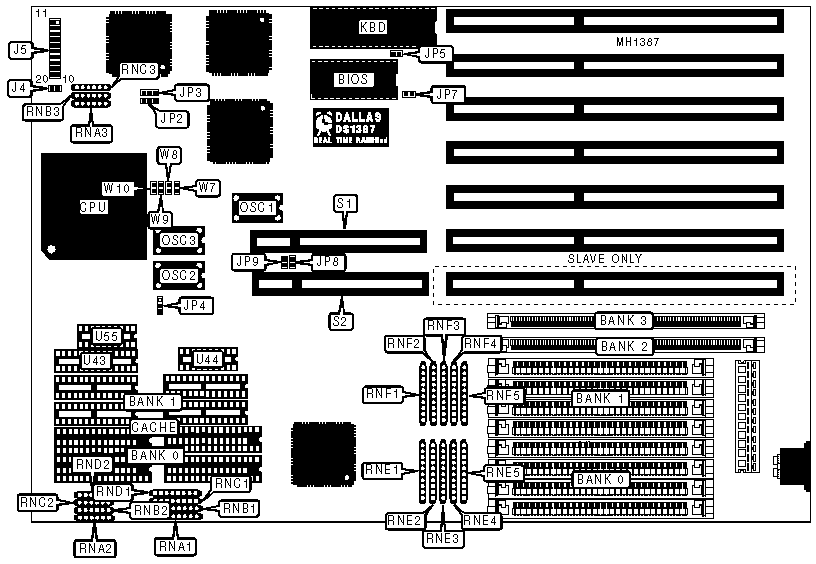
|
Processor |
80486SX/80487SX/80486DX/ODP487SX/80486DX2 |
|
Processor Speed |
20/25/33/40(internal)/50(internal)/50/66(internal)MHz |
|
Chip Set |
OPTI |
|
Max. Onboard DRAM |
128MB |
|
SRAM Cache |
64/128/256/512KB |
|
BIOS |
AMI |
|
Dimensions |
220mm x 240mm |
|
I/O Options |
32-bit VESA card slot (2) |
|
NPU Options |
None |
|
CONNECTIONS | |||
|
Purpose |
Location |
Purpose |
Location |
|
IDE interface LED |
J4 |
Reset switch |
J5 pins 9 and 19 |
|
Speaker |
J5 pins 1-4 |
IDE interface LED |
J5 pins 10 and 20 |
|
Turbo switch |
J5 pins 7 and 17 |
32-bit VESA card (2) |
S1 & S2 |
|
Turbo LED |
J5 pins 8 and 18 | ||
|
USER CONFIGURABLE SETTINGS | |||
|
Function |
Jumper |
Position | |
| » |
Monitor type select color |
JP5 |
closed |
|
Monitor type select monochrome |
JP5 |
open | |
| » |
Channel ready select normal |
JP7 |
open |
|
Channel ready select EXRDY signal generated |
JP7 |
closed | |
|
DRAM CONFIGURATION | ||||||
|
Size |
Bank 0 |
Bank 1 |
Bank 2 |
Bank 3 |
RNE1-RNE5 |
RNF1-RNF5 |
|
4MB |
(4) 1M x 9 |
NONE |
NONE |
NONE |
closed |
open |
|
4MB |
NONE |
NONE |
(1) 1M x 36 |
NONE |
open |
closed |
|
8MB |
(4) 1M x 9 |
(4) 1M x 9 |
NONE |
NONE |
closed |
open |
|
8MB |
NONE |
NONE |
(1) 1M x 36 |
(1) 1M x 36 |
open |
closed |
|
12MB |
(4) 1M x 9 |
(4) 1M x 9 |
(1) 1M x 36 |
NONE |
closed |
open |
|
12MB |
(4) 1M x 9 |
NONE |
(1) 1M x 36 |
(1) 1M x 36 |
open |
closed |
|
16MB |
(4) 1M x 9 |
(4) 1M x 9 |
(1) 1M x 36 |
(1) 1M x 36 |
closed |
open |
|
16MB |
(4) 4M x 9 |
NONE |
NONE |
NONE |
closed |
open |
|
16MB |
NONE |
NONE |
NONE |
NONE |
closed |
open |
|
20MB |
(4) 4M x 9 |
(4) 1M x 9 |
(1) 4M x 36 |
NONE |
open |
closed |
|
20MB |
NONE |
NONE |
(1) 4M x 36 |
(1) 1M x 36 |
open |
closed |
|
24MB |
(4) 4M x 9 |
(4) 1M x 9 |
(1) 1M x 36 |
NONE |
closed |
open |
|
28MB |
(4) 4M x 9 |
(4) 1M x 9 |
(1) 1M x 36 |
(1) 1M x 36 |
closed |
open |
|
32MB |
(4) 4M x 9 |
(4) 4M x 9 |
NONE |
NONE |
closed |
open |
|
32MB |
NONE |
NONE |
(1) 4M x 36 |
(1) 4M x 36 |
open |
closed |
|
36MB |
(4) 4M x 9 |
(4) 4M x 9 |
(1) 1M x 36 |
NONE |
closed |
open |
|
36MB |
(4) 4M x 9 |
NONE |
(1) 4M x 36 |
(1) 4M x 36 |
open |
closed |
|
40MB |
(4) 4M x 9 |
(4) 4M x 9 |
(1) 1M x 36 |
(1) 1M x 36 |
closed |
open |
|
40MB |
(4) 4M x 9 |
NONE |
(1) 1M x 36 |
(1) 4M x 36 |
open |
closed |
|
48MB |
(4) 4M x 9 |
(4) 4M x 9 |
(1) 4M x 36 |
NONE |
closed |
open |
|
48MB |
(4) 4M x 9 |
NONE |
(1) 4M x 36 |
(1) 4M x 36 |
open |
closed |
|
52MB |
(4) 4M x 9 |
(4) 1M x 9 |
(1) 4M x 36 |
(1) 4M x 36 |
closed |
open |
|
64MB |
(4) 4M x 9 |
(4) 4M x 9 |
(1) 4M x 36 |
(1) 4M x 36 |
closed |
open |
|
128MB |
(4) 16M x 9 |
(4) 16M x 9 |
NONE |
NONE |
closed |
open |
|
SRAM RESISTOR CONFIGURATION | ||||
|
Size |
RNA1/RNA2 |
RNB1/RNB2 |
RNC1/RNC2 |
RND1/RND2 |
|
64KB |
closed |
open |
open |
open |
|
128KB |
open |
closed |
open |
open |
|
256KB |
open |
open |
closed |
open |
|
512KB |
open |
open |
open |
closed |
|
SRAM CONFIGURATION | ||||
|
Size |
Cache SRAM |
Location |
TAG(U43) |
TAG(U44 & U55) |
|
64KB |
(8) 8K x 8 |
Banks 0 & 1 |
(1) 8K x 8 |
(2) 16K x 1 |
|
128KB |
(4) 32K x 8 |
Bank 0 |
(1) 8K x 8 |
(2) 16K x 1 |
|
256KB |
(8) 32K x 8 |
Banks 0 & 1 |
(1) 32K x 8 |
(2) 16K x 1 |
|
512KB |
(4) 128K x 8 |
Bank 0 |
(1) 32K x 8 |
(2) 64K x 1 |
|
CPU JUMPER CONFIGURATION | |||
|
CPU |
RNA3 |
RNB3 |
RNC3 |
|
80486DX2 |
closed |
open |
open |
|
ODP486SX |
open |
closed |
open |
|
80486DX |
closed |
open |
open |
|
80487SX |
open |
closed |
open |
|
80486SX |
open |
open |
closed |
|
CPU SPEED JUMPER CONFIGURATION | |||||||||
|
CPU |
JP2 |
JP3 |
JP4 |
JP8 |
JP9 |
W7 |
W8 |
W9 |
W10 |
|
20MHz |
1 & 2 |
1 & 2 |
2 & 3 |
open |
open |
open |
closed |
open |
open |
|
25MHz |
1 & 2 |
1 & 2 |
2 & 3 |
open |
open |
open |
open |
closed |
open |
|
33MHz |
1 & 2 |
2 & 3 |
2 & 3 |
open |
open |
closed |
open |
open |
open |
|
40(internal)MHz |
1 & 2 |
1 & 2 |
2 & 3 |
open |
open |
open |
closed |
open |
open |
|
50(internal)MHz |
1 & 2 |
1 & 2 |
2 & 3 |
open |
open |
open |
open |
closed |
open |
|
50MHz |
2 & 3 |
2 & 3 |
1 & 2 |
closed |
closed |
open |
open |
closed |
open |
|
66(internal)MHz |
1 & 2 |
2 & 3 |
2 & 3 |
open |
open |
open |
open |
open |
closed |
|
Note:JP8 and JP9 are VESA bus speed select. W7 - W10 are clock source jumpers.
| |||||||||